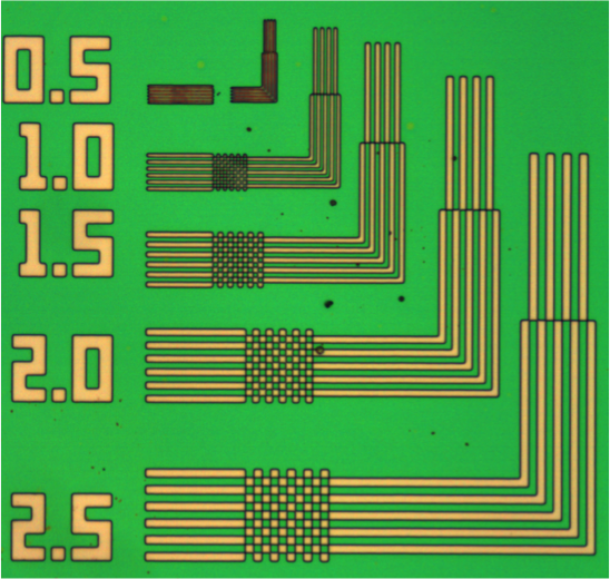
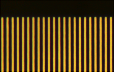
Samples:

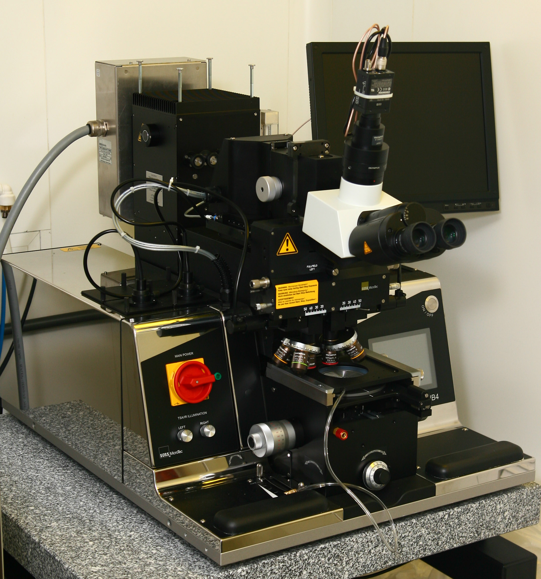
Alignment of photomask with wafer and resist exposition for contact lithography.
Manufacturer: Suss MicroTec, Germany
Year: 2007
Location: 213
| Contact lithography modes: | |
| soft contact | |
| hard contact | |
| rough vacuum contact | |
| vacuum contact | |
| gap printing: | 0—50 µm |
| Spatial resolution: | up to 0.6 µm |
| Wafers: | Si, GaAs, LiNbO3 and others |
| Maximum wafer size: | 100 mm (4”) |
| Maximum bit size: | from 10 x 10 mm2 |
The equipment is installed in the clean room (class 100) intended for contact photolithography.