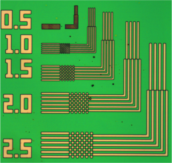
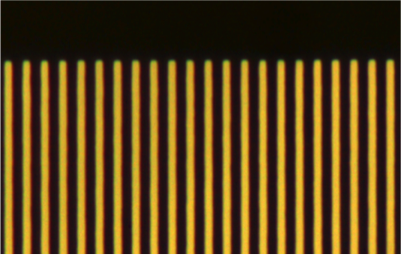
Примеры:

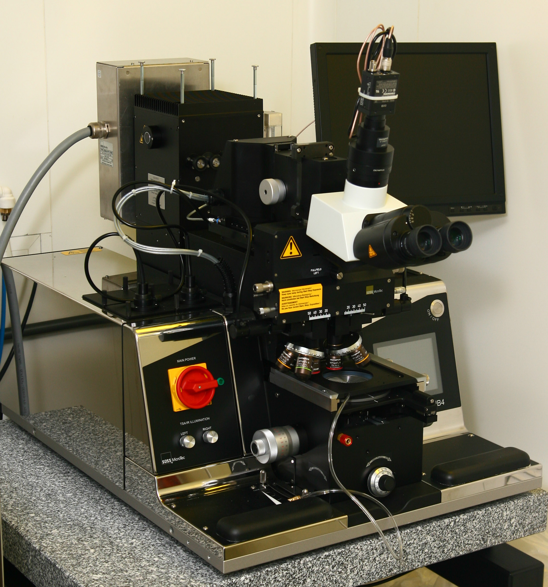
В составе Комплекса оборудования для фотолитографии
Совмещение фотошаблона и пластины, а также экспонирование фоторезиста для контактной литографии. Система экспонирования позволяет работать на длинах волны 250, 300 и 400 нм без замены лампового блока.
Производитель: Suss MicroTec, Германия
Год выпуска: 2007
Комната: 213
| Режимы контактной литографии | |
| - мягкий контакт | |
| - жесткий контакт | |
| - низковакуумный контакт | |
| - вакуумный контакт | |
| - контакт с зазором в диапазоне | от 0 до 50 мкм |
| Предельное разрешение при вакуумном контакте | 0.6 мкм |
| Подложки | кремний, GaAs, GaN, LiNbO3 и другие |
| Размер | |
| - кусочки | от 10х10 мм2 |
| - пластины | до 100 мм в диаметре |
Оборудование размещено в чистом помещении класс ГОСТ ИСО 5